ITEM
Interfacing Technologies for Edge Microsystems
Interfacing Technologies for Edge Microsystems
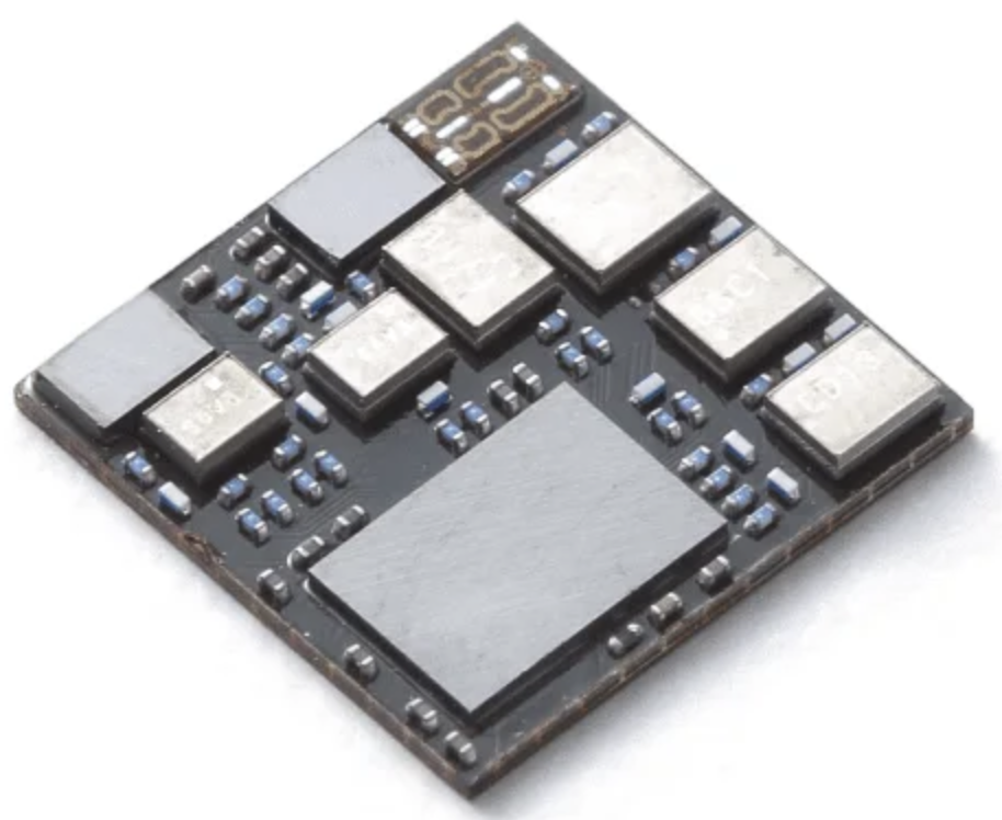
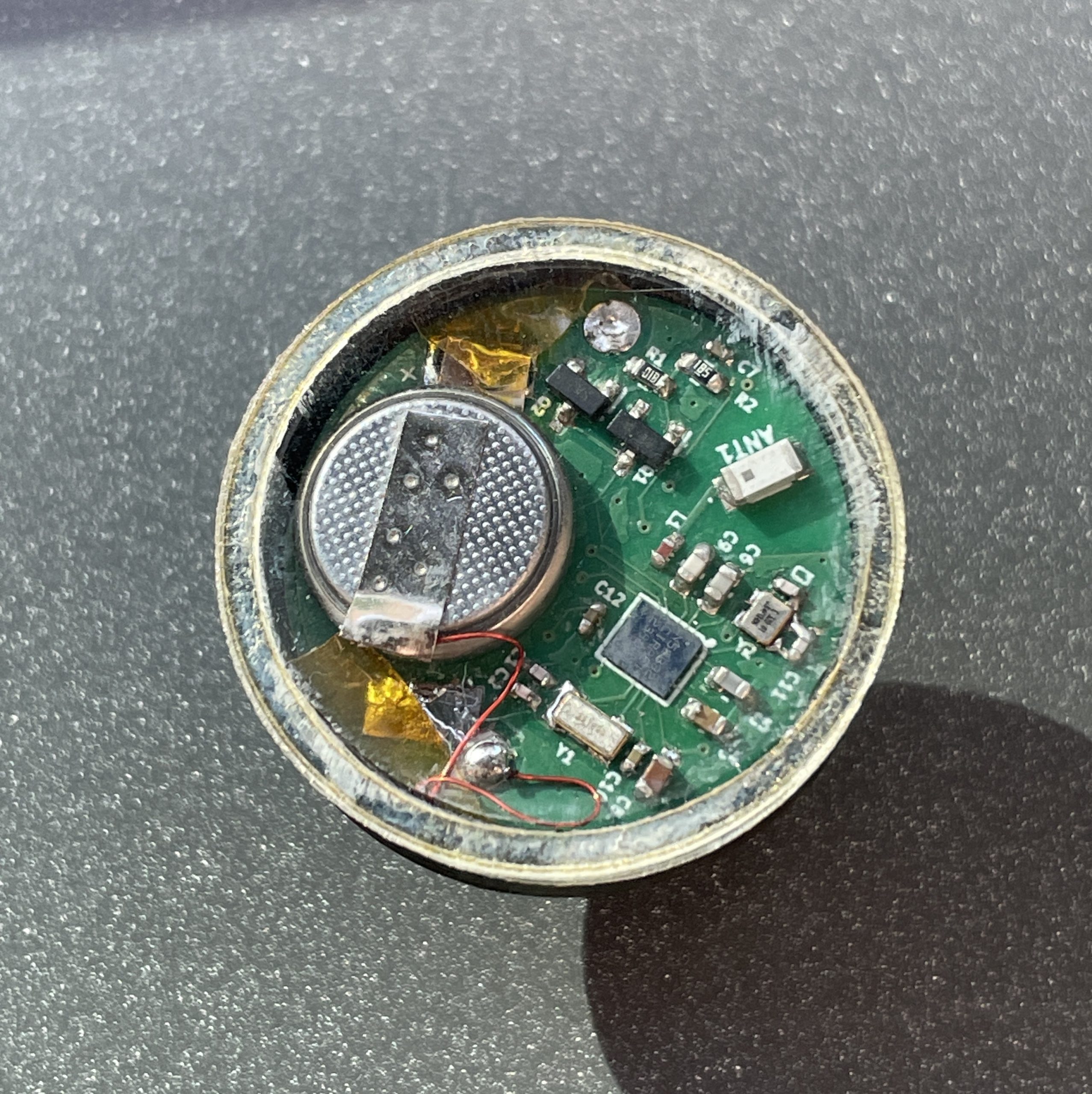
System-in-Package (SiP) is an advanced packaging technology that integrates multiple integrated circuits along with other components such as capacitors, resistors - and even antennas, into a single module. Unlike a System-on-Chip (SoC), where all components are integrated onto a single piece of silicon, SiP combines individually manufactured and tested chips into one package. This approach offers significant advantages, particularly in terms of miniaturization, performance, and cost-effectiveness.
SiP technology enables the creation of highly compact and complex electronic systems, making it ideal for applications in many and different fields. By allowing for the integration of diverse functionalities—like processors, memory, and sensors—from different manufacturing processes within a single package, SiP can also improve overall system performance and reduce power consumption due to shorter interconnections. Furthermore, it offers greater flexibility in design and can accelerate time-to-market by leveraging proven, off-the-shelf components.
In addition to these benefits, SiP technology is also considered more environmentally friendly compared to SoC. This is because SiP allows for the individual testing of sub-components before they are integrated into the final assembly. This ability to identify and eliminate defective parts before the complete package is manufactured significantly reduces waste in the production process, contributing to a more sustainable approach in electronics manufacturing.
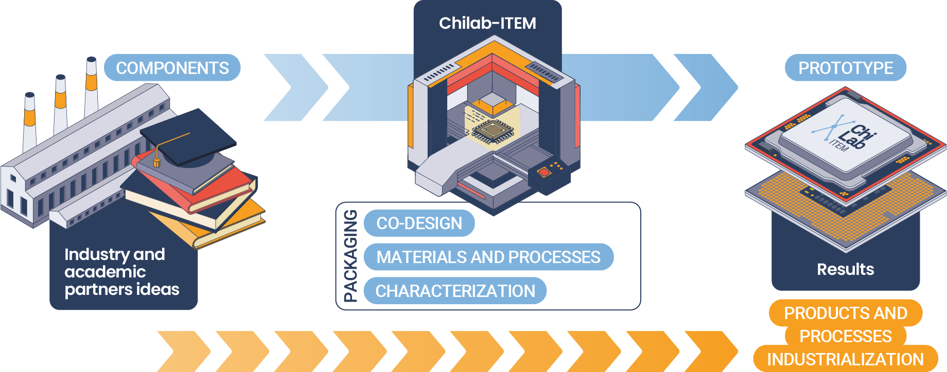
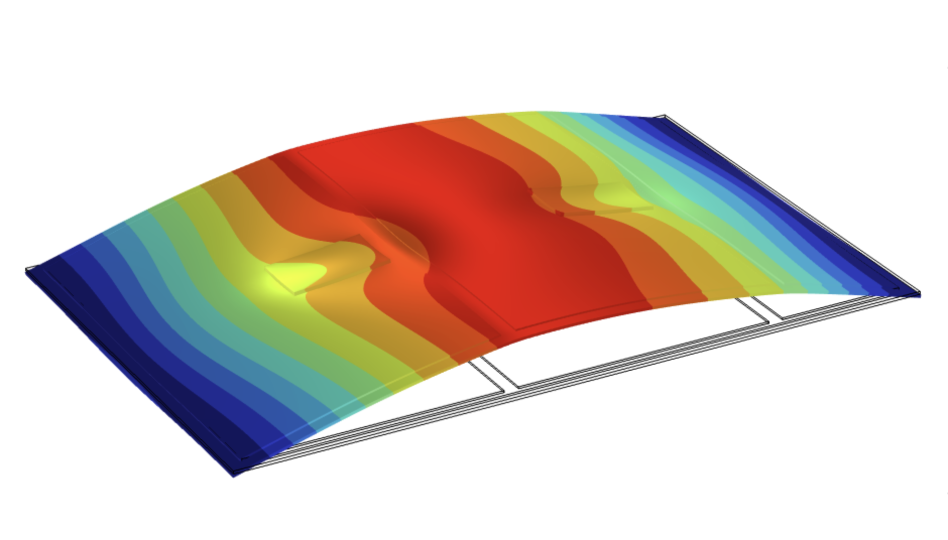
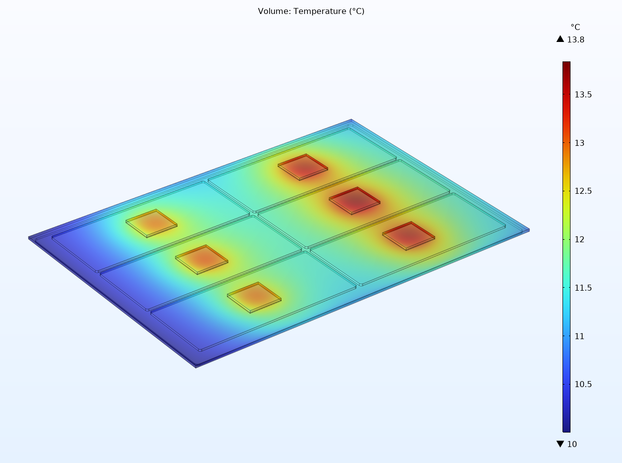
Co-design represents an integrated and iterative methodology that comprehensively addresses the design and optimization of all electronic system components, including their interconnections with the surrounding physical environment. This methodology is paramount, particularly with the escalating demand for integration in advanced devices such as the aforementioned Systems in Package (SiP).
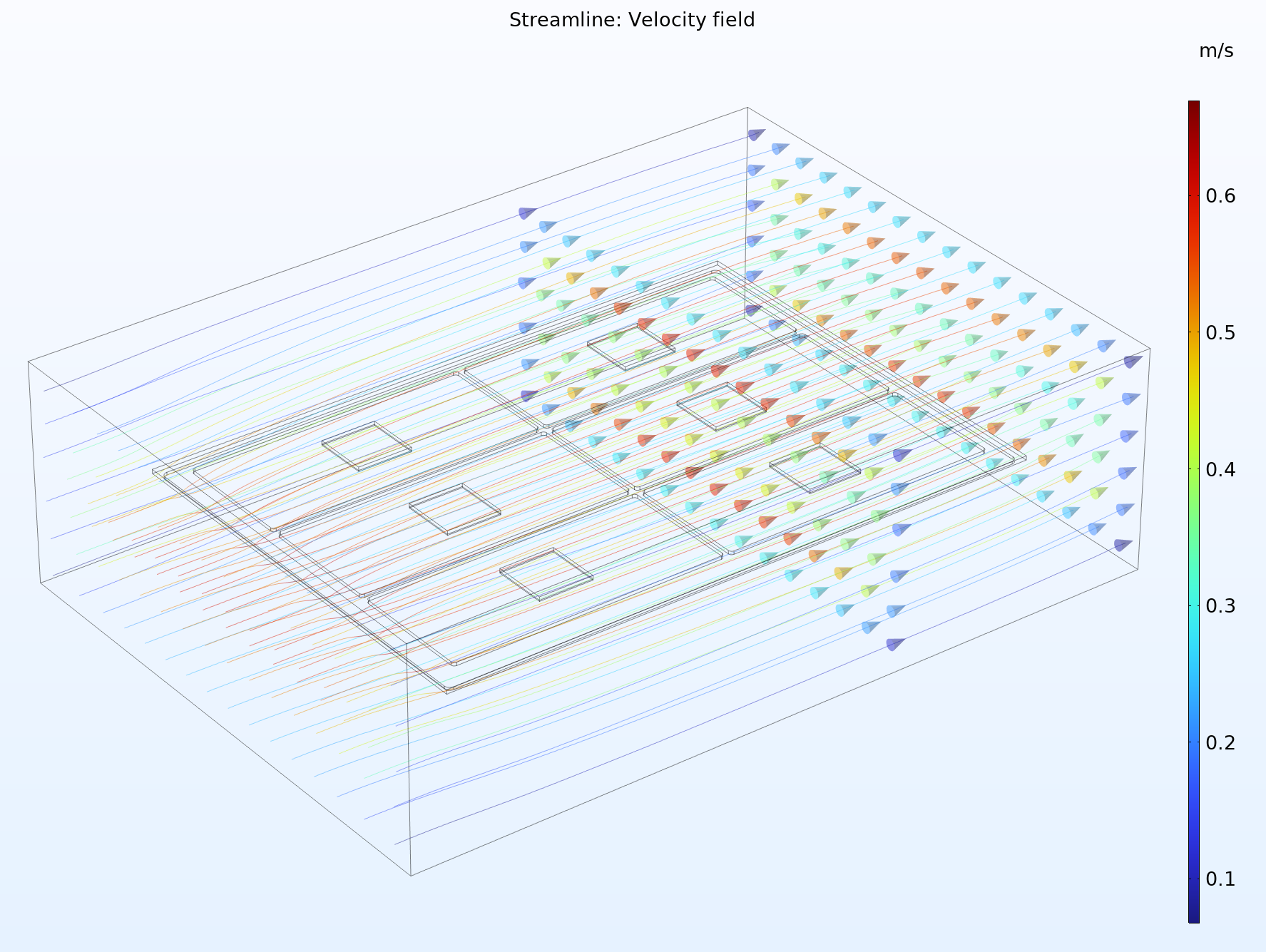
At Chilab-ITEM, we specialize in leveraging cutting-edge simulation tools, including Multiphysics Finite Element Method (FEM) simulation, to drive innovation in co-design. Our ever-growing experience allows us to create highly accurate virtual models of devices, enabling precise prediction and in-depth analysis of their performance across various domains. We proactively identify and mitigate potential issues such as component failures, signal integrity degradation, and thermal hotspots early in the design cycle by meticulously studying optical, mechanical, electromagnetic, and thermal behaviors.
The power of multiphysics interfaces within our simulation software allows for the simultaneous evaluation of multiple interacting phenomena. This comprehensive approach ensures the development of more robust, reliable, and efficient devices, ultimately accelerating time-to-market and significantly reducing development costs. Our computational capabilities position us as an invaluable partner throughout both the design and fabrication processes of your devices. We achieve this by developing advanced simulations of the device itself, being able to fully characterize the intricate behavior of materials within a multiphysics domain and therefore validating our simulations within our own laboratories.
We invite you to partner with Chilab-ITEM to unlock the full potential of your SiP innovations. How can our co-design expertise and advanced simulation capabilities support your next project?
Since SiP involves encapsulating diverse elements—including passive and active components, MEMS, and optical elements—within a single package, the choice of materials for both packaging and internal components, such as metals, polymers, and ceramics, is essential for ensuring device reliability and thermal stability, and the overall functionality of the device.
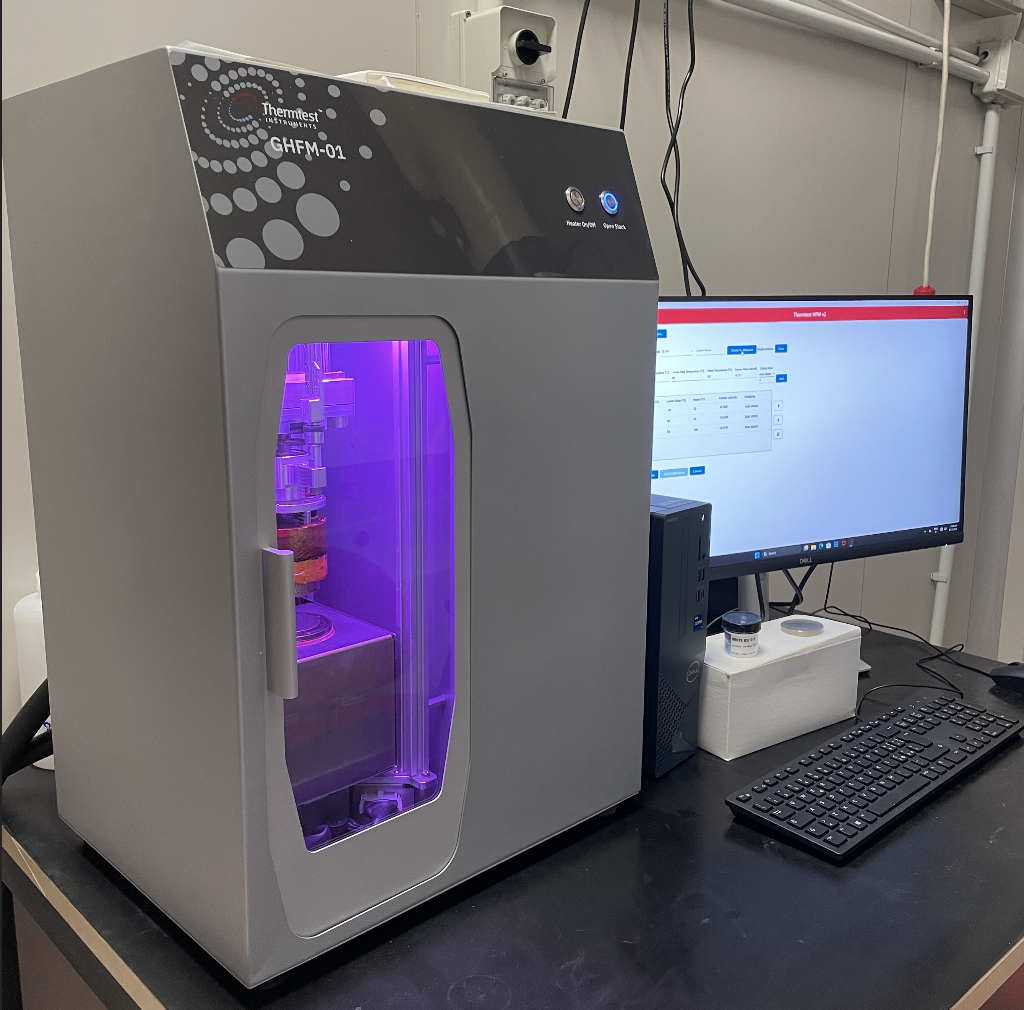
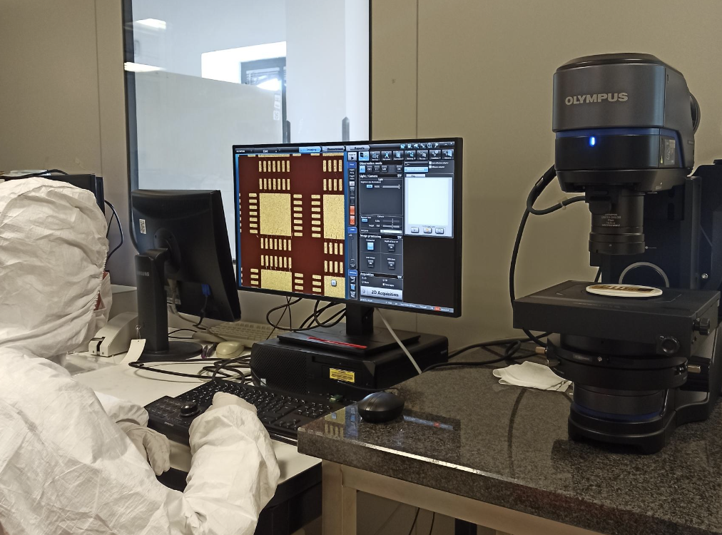
At Chilab-ITEM we have machinery able to:
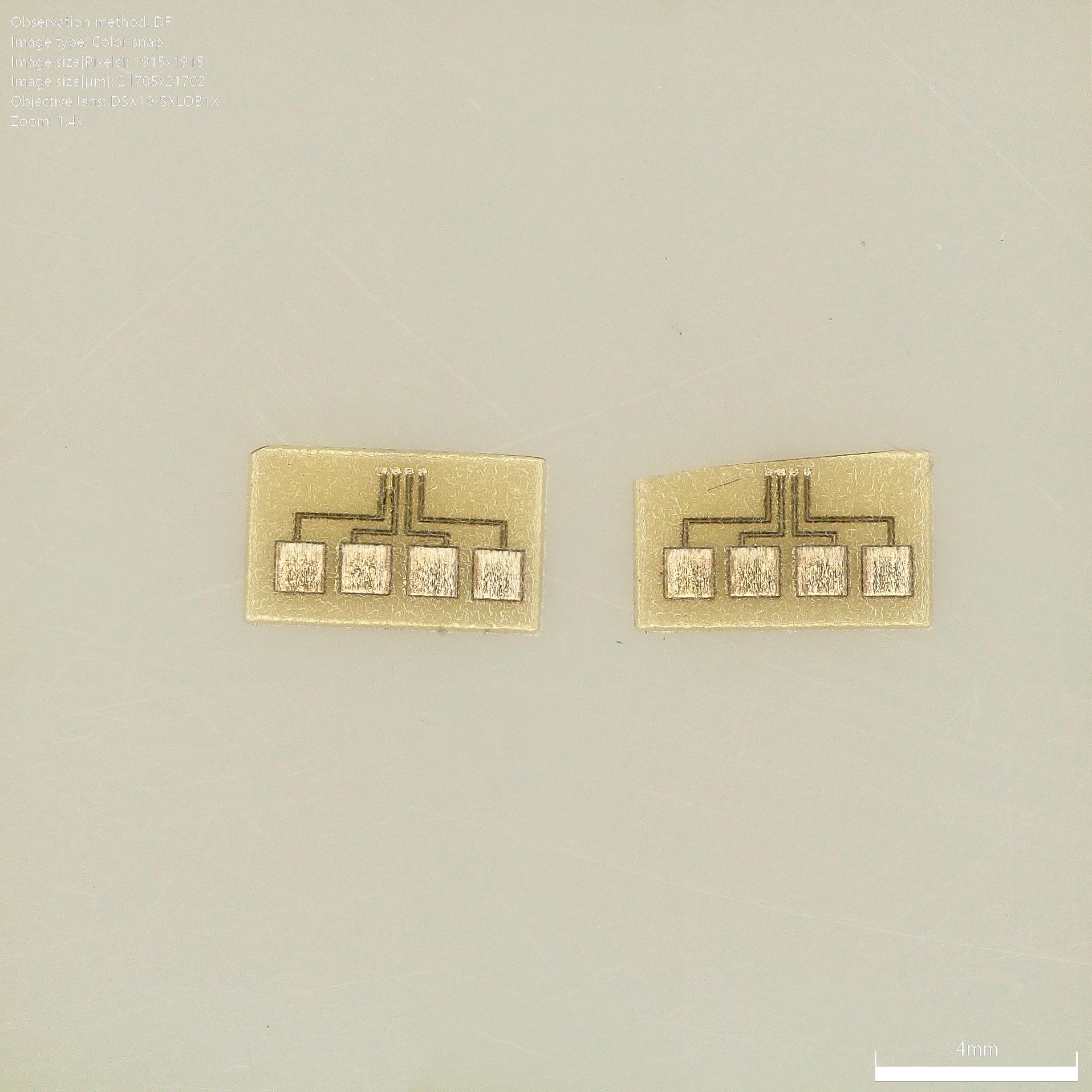
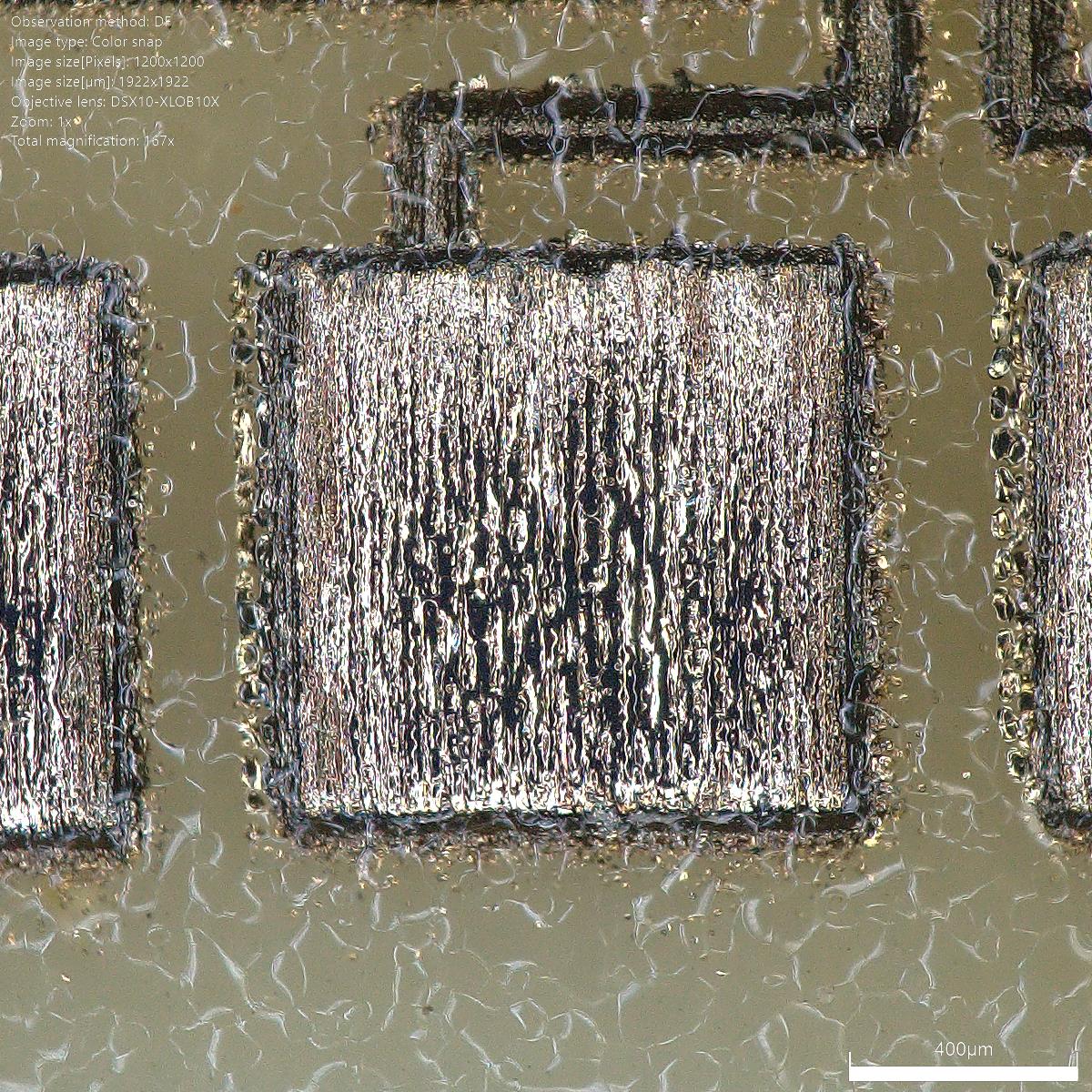
The thermal, morphological and opto-electronic characterization of innovative prototypes, usually focused on the evaluation of the packaging abilities to protect the bare die in a SiP from environmental and operational disturbances, is one of the last steps in the investigation of the efficiency of System-in-Package device, by analysing integration within system components.
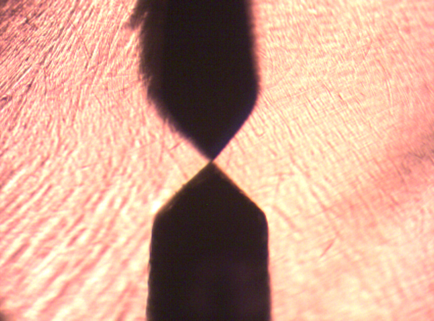
Characterization techniques use advanced instruments able to perform sophisticated analysis such as a climate chamber, a digital microscope, a profilometer, and a thermal conductivity test machine. At the same time, the validation of the prototype must be assessed, thanks to electrical or optic characterization. The ultimate goal is to provide a complete evaluation of the performance and reliability of advanced packaging prototypes, focusing on increasing thermal dissipation, miniaturization, and device reliability.